Aaron's Homepage Forum
Home | Profile | Register | Active Topics | Members | Search | FAQ
Username:
Password:
Save Password
Forgot your Password?

 All Forums
 Electronics
 Basic Electronics
 CMOS NAND gate 4011
 New Topic  Reply to Topic
 Printer Friendly
Author Previous Topic Topic Next Topic  

nghtcrwlr
New Member

1 Posts

Posted - Oct 07 2009 :  10:40:42 AM  Show Profile  Reply with Quote
Hello
i have recently seen a capacitive touch circuit from http://www.aaroncake.net/CIRCUITS/touch.asp

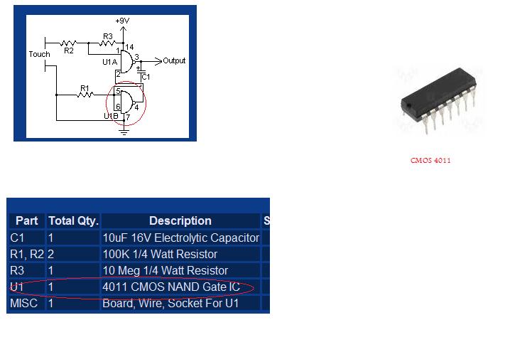
There a CMOS NAND Gate 4011 is used. and in the circuit diagram 4 terminals are connected. but the actual components has 7 +7 leads on each side. Can anyone please explain me the circuit.
Thanks


Download Attachment: CMOS.jpg
37.76 KB

audioguru
Nobel Prize Winner

Canada
4218 Posts

Posted - Oct 07 2009 :  12:36:13 PM  Show Profile  Reply with Quote
You should never leave inputs on a Cmos logic IC not connected. Connect the unused inputs to 0V.
look at its datasheet to see which pins are the unused inputs.
Go to Top of Page

Darkthero
Apprentice

USA
51 Posts

Posted - Nov 02 2009 :  11:54:12 PM  Show Profile  Reply with Quote
i checked the data sheet. and some other circuit that use the same chip. ot is fine to not use the other pins. so just wire it like the schematic says
Go to Top of Page

Darkthero
Apprentice

USA
51 Posts

Posted - Nov 02 2009 :  11:57:35 PM  Show Profile  Reply with Quote
oh btw U1A and U1B is the same chip so connect 1 2 3 and 5 6 4 7 to your NAND Gate 4011
Go to Top of Page
  Previous Topic Topic Next Topic  
 New Topic  Reply to Topic
 Printer Friendly
Jump To:
Aaron's Homepage Forum © 1995-2020 AARONCAKE.NET Go To Top Of Page
This page was generated in 0.06 seconds. Snitz Forums 2000