| Author |
 Topic Topic  |
|
pebe
Nobel Prize Winner

United Kingdom
1078 Posts |
 Posted - Apr 08 2009 : 08:51:05 AM Posted - Apr 08 2009 : 08:51:05 AM


|
| Leave it out of the circuit. |
 |
|
|
kivdenn
Nobel Prize Winner
Uganda
535 Posts |
Posted - Apr 10 2009 : 06:58:14 AM
|
| Thanks let me try it out. Dennis |
|
|
|
kivdenn
Nobel Prize Winner
Uganda
535 Posts |
Posted - Sep 02 2009 : 08:53:34 AM
|
I have failed to get the CA3140 in my country, is there a substitute for the same IC ? Thanks
Dennis |
|
|
|
pebe
Nobel Prize Winner
United Kingdom
1078 Posts |
Posted - Sep 02 2009 : 10:52:16 AM
|
Any op-amp with a high input impedance such as JFET or CMOS can be used.
TL081, TL061, OPA42, OPA227 or LF351 should be suitable. |
|
|
|
kivdenn
Nobel Prize Winner
Uganda
535 Posts |
Posted - Sep 03 2009 : 09:11:15 AM
|
| Its like we are using pins 2,3,4,6 and seven, what hapens to other pins like 1,5 and 8? Thanks |
|
|
|
pebe
Nobel Prize Winner
United Kingdom
1078 Posts |
Posted - Sep 03 2009 : 1:47:41 PM
|
Pins 1&5 are offset null pins. On the CA3140 pin 8 is the 'strobe' but on other op-amps may not be used.
Leave all 3 pins unconnected. |
|
|
|
kivdenn
Nobel Prize Winner
Uganda
535 Posts |
Posted - Sep 04 2009 : 05:41:46 AM
|
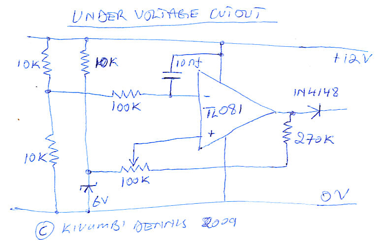
Hi Pebe I want to incorporate your LVD circuit into my inverter circuit and I have tried to draw a full diagram of the LVD ciercuit. I want to know if every thing on it is correct? Because in your diagram you left out the 6V zener and the half battery supply and now i have tried to include them.Please check and see if am correct.
Is it ok for me also to use a 10nf ceramic capacitor because it apears that you used an electrolyte one. Also if I want to include an LED to iluminate when the LVD is active ( When the battery is low), where do I connect it? Thanks
Dennis
Download Attachment:  Full undervoltage cutout circuit.jpg Full undervoltage cutout circuit.jpg
139.61�KB
 |
Edited by - kivdenn on Sep 04 2009 05:48:41 AM |
|
|
|
kivdenn
Nobel Prize Winner
Uganda
535 Posts |
Posted - Sep 05 2009 : 09:16:06 AM
|
| Please some body help me with this. Thanks |
|
|
|
pebe
Nobel Prize Winner
United Kingdom
1078 Posts |
Posted - Sep 05 2009 : 6:10:04 PM
|
| There are a couple of errors in your circuit. If you can just bear with me until my weekened visitors have gone, I will look up my original circuit. |
|
|
|
kivdenn
Nobel Prize Winner
Uganda
535 Posts |
Posted - Sep 07 2009 : 01:42:01 AM
|
Another thing is that I failed to get LMC555 CMOS IC all I can get is the NE555 bipolar IC is there a way I can substitute this one or can any saw tooth oscilator work in place of the LMC55 circuit? If so please advise me on the right alternative saw tooth oscilator circuit to use. Thanks
Dennis |
|
|
|
pebe
Nobel Prize Winner
United Kingdom
1078 Posts |
Posted - Sep 07 2009 : 07:16:37 AM
|
I have rechecked and your circuit is OK as it is. By varying the 100K pot you can get it to cutoff anywhere between 12V and 8.7V
I'll check on the 555 and come back to you. |
|
|
|
kivdenn
Nobel Prize Winner
Uganda
535 Posts |
Posted - Sep 07 2009 : 10:20:08 AM
|
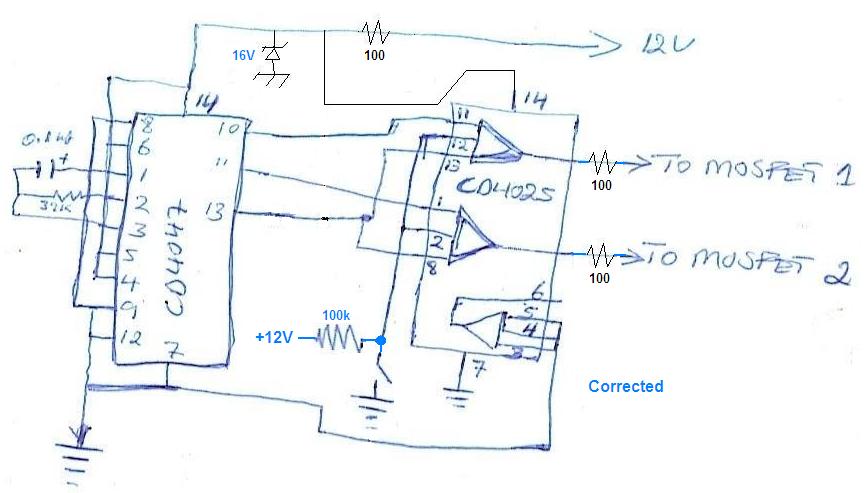
How do I apply this LVD circuit to this oscilator circuit? Do I still conect it to the resset pin of CD4025? If so what happens to the 100k pull up resistor and the on/off switch? Alternatively how can i place a relay switch so that it does the on/off switch? Please help me with this because the other one failed as i cant get the LMC555 IC. Thanks
Download Attachment: CD4047 & CD4025 oscilator.jpg
46.8�KB
 |
Edited by - kivdenn on Sep 07 2009 10:22:45 AM |
|
|
|
pebe
Nobel Prize Winner
United Kingdom
1078 Posts |
Posted - Sep 07 2009 : 10:47:05 AM
|
To apply the LDV to your circuit:-
Remove the 100K resistor and switch from pins2&12 of the CD4025.
Remove the diode from the TL081 of the LDV.
Connect the output of the TL081 to pins2&12 of the CD4025.
Have you discarded the 555 circuit, so you don't need an answer?
|
|
|
|
kivdenn
Nobel Prize Winner
Uganda
535 Posts |
Posted - Sep 08 2009 : 06:27:38 AM
|
| Eeeee!!! I need it so much infact if I can only get the substitute to the LMC555 Cmos timer or an equivalent circuit am ready to continue with it. With the modification of the circuit to include the LVD, wont my mosfets blow if I remove +12V from the ICs and leave the transformer connected to the battery? I mean can it still be used as an inverter/cherger as I had explained to you before? Thanks |
|
|
|
pebe
Nobel Prize Winner
United Kingdom
1078 Posts |
Posted - Sep 08 2009 : 07:24:12 AM
|
With both the LM555 and LMC555 the voltage swing on the charging capacitor is the same, ie. 1/3 to 2/3 supply voltage. So the LM555 can be used as a replacement. But the output swing of the LM555 is less than the LMC555 so the circuit will run a little slower. You may need to reduce the value of R1 a bit to compensate.
CD4025 is a pack of triple input NOR gates. When the LDV operates, TL081 output takes pins2 & 12 high and the gates are activated. Both their outputs go low cutting off the FETs. |
|
|
|
Topic |
|
 CD4047 & CD4025 oscilator.jpg